公司简介: A world-class technology company, Advantest is the leading producer of automatic test equipment (ATE) for the semiconductor industry and a premier manufacturer of measuring instruments used in the design and production of electronic instruments and systems. Its leading-edge systems and products are integrated into the most advanced semiconductor production lines in the world. The company also focuses on R&D for emerging markets that benefit from advancements in nanotech and terahertz technologies, and has introduced multi-vision metrology scanning electron microscopes essential to photomask manufacturing, as well as a groundbreaking 3D imaging and analysis tool. Founded in Tokyo in 1954, Advantest established its first subsidiary in 1982, in the USA, and now has subsidiaries worldwide. More information is available at www.advantest.com.
产品推荐


新闻动态

同是12英寸芯片厂,从打桩到量产粤芯比博世快了2年
据粤芯半导体官方消息,面对日益增长的终端运用需求,博世已有的6英寸和8英寸芯片工厂不足以满足自身产品线对芯片的需求,进而把眼光投向于规模经济更高的12英寸芯片生产线,该

高通:骁龙X55已被全球超过30家厂商采用
10月14日,高通全资子公司高通技术宣布,骁龙X55 5G调制解调器及射频系统已被全球超过30家OEM厂商采用,以支持商用5G固定无线接入(FWA)CPE终端自2020年开始发布。与高通合作的OEM厂商

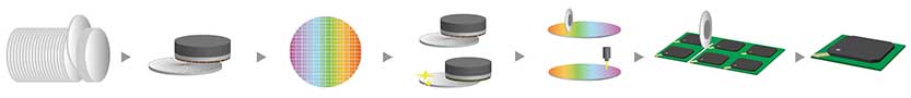
国内新布局多座12英寸晶圆厂
日前,闻泰12英寸车规级功率半导体自动化晶圆制造中心项目宣布签约落户上海,该消息备受业界关注,国内将再添一座12英寸晶圆厂。近年来,随着国家大力发展集成电路,国内12英寸
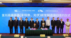
总投资10.6亿元 上海釜川高端装备研发制造项目落地无锡
近日,江苏无锡锡山区东港镇人民政府与上海釜川自动化设备有限公司(以下简称 上海釜川 )举行签约仪式。从洽谈到落地仅用20天,总投资10.6亿元的釜川高端装备(半导体、光伏)研

意法半导体制造出首批200mm碳化硅晶圆!
本文《意法半导体制造出首批200mm碳化硅晶圆!》,重点介绍芯片制造/封测细分领域相关信息,787字涉及芯片,意法半导体,晶圆制造相关信息。